tiistai 2. huhtikuuta 2019

Modifying an FM radio

TL;DR I tried to modify an FM radio that only goes up to 108 MHz to receive weather satellites at 138 MHz. That failed, but I learned thing or two on the way.

Introduction

I read about receiving weather satellites with PC sound card and a modified radio many years ago, and since that time I've always wanted to do that. Today it is rather simple to do with very inexpensive software defined radios (SDRs), but using pre-built components is only half the fun.

The weather satellites I talk about transmit at 137 to 138 MHz using FM modulation. The easy way to receive that is to use a radio scanner and connect it to PC using the sound card line input and the software in previous link decodes to images. A powerful antenna may be needed, but that is just details ;)

Radio scanners tend to be quite expensive compared to normal FM radio receivers. Where I live, the FM radio band goes from about 88 MHz to 108 MHz, so quite close to what I needed. I decided to try and modify an existing radio to reach the required band.


Selecting a radio

I looked at the most inexpensive receivers and especially one that looked to have an analog tuning mechanism. I thought that one with analog tuning would have some LC tuning circuit, which I could modify to an upper frequency to extend the band upwards. I assumed that ones with digital tuning (e.g. buttons to tune up and down) might be hard to modify.

I ended up buying a Prego FM/AM radio which had analog potentiometer style tuning and volume. Below is a picture of what the radio looks like.


Opening it up

I opened the radio and looked at the PCB. There was no obvious tuning circuit (coils and capacitors) or even crystal oscillators visible on the board.

On the top side there was few IC circuits and on the bottom side just one. The bottom side one was a power amplifier driving the speaker, so what I wanted was one on the top side.

On the top side there was some regulators and interestingly a EEPROM of type L24C02B. This turned out to be important but I didn't know it yet.

The radio chip was under some plastic, protecting it from the mains transformer. The type of the radio receiver is KTmicro KT0922. Luckily I found datasheet for it.

Reworking SMD components

In all electronics projects I have done, there has always been few errors. Component value errors are easy to solve by just changing the component, but wrong components or wrong component pinouts are more difficult.

I think I've never managed to do any project where there wasn't any issues with component pinouts. Either some pins are swapped by accident, or I need to use other component (due to design error) which has different pinout.

In this post I will show how I work around wrong pinouts in SMD components.

Backgroud

Some time ago I designed a class D (subwoofer) amplifier . In the circuit I used a high and low side driver to drive the output H-bridge transistors. I selected ADP3120A from OnSemi for the driver, since I thought it would work fine with the 24 V power supply I was going to use.

However it turned out that the voltage rating of the component was not enough, and I needed to change the component. I could not find any pin-to-pin compatible replacement with higher voltage, so I decided to use a IR2104 from Infineon, which is logically compatible, and work my way around the pin differences.

The plan

The pinout for each chip is shown below. As can be seen, only 3 pins are directly compatible, marked with red squares.

Comparison of component pinouts
The plan how to fix the pin incompatibility is to solder the new chip in place with those 3 pins. The other ones will be lifted up with tweezers and then soldered to wherever the pins would go with jumper wires.

To ease the process, I checked the schematic and selected the components that I will solder the jumper wires to. In the following figure different colors indicate where the connection will be made. The blue numbers are the pinout of the new component, while the red numbers (originals) are from the old chip.

Planning of jumper connections in schematic
After this, I checked the layout drawing and marked the correct solder pads there also, with same colors.
Layout drawing with connections marked

After this step, it is quite straightforward to do the soldering.

Implementation

First, before soldering anything, I carefully bent up the pins that were not meant to be soldered down. Then using the 3 pins that were compatible between both chips, I soldered the chip to board.

After the chip was down, I put small pieces of polyimide tape under the lifted pins to prevent accidental solder bridges.

Pins lifted and small pieces of tape added under them

Then I measured pieces of thin single-strang wire-wrapping wire from each pin to the correct pads. I first soldered the pieces, one at a time, to the other pad (resistor pad, diode pad or similar larger pad) first, and then carefully routed the wire to the component pin. Adding a very tiny amount of solder, I then soldered the free end to the lifted component pin.

First jumper wire soldered to pad and pin
After the first jumper wire, I continued with other wires. Always measuring the length, soldering first to the other component, then carefully bending the wire into place and then soldering to component pin.

It is better to solder the wires first to a larger component because then the wire can be bent more safely without risk of breaking the component pin or the tiny solder connection between the pin and the wire.

Also with the wire I used, I found it easiest to not try to strip the wire with any pliers, but instead touch the end of the wire with hot soldering iron. This caused the insulator to shrink and expose just enough of the wire to allow soldering it.

It took some time to solder all the connections, but here is picture of the finished rework.
Finished rework

Maybe not the best soldering job I've done, but it does the trick. A good idea is to add some hot glue or tape to fix the wires into place then.

Happy soldering!

sunnuntai 6. tammikuuta 2019

STM32 remote debugging with Raspberry PI Zero W, OpenOCD and Eclipse

I'm doing an electronics project which uses a STM32F103RF microprocessor, and I needed a way to flash my own firmware into the micro and also a way to debug it. I don't have any special programmer for the micro, nor any generic JTAG adapters or such, but luckily I read online (e.g. this guide or another guide) that it should be possible to use a Raspberry PI as a JTAG/SWD (single wire debug) interface for fashing and debugging the STM32 micros.

However, about all the guides seemed to use the larger Raspberry Pis, like A or 3, and I had only the wireless Raspberry Pi zero W model. The guides didn't work out directly, but luckily I got it to work in the end and here I describe how.

Another plus side is that the zero W uses wifi connection, so I got wireless debugging over wifi, which is great since my project is mains powered, and now I can flash and debug safely without risk of electic shock!

STM32 connection

I designed in a very simple debug connection to the project. The SWD pins are routed directly from the processor to the debug connector, together with the reset pin. Following figures show the schematic I used for the debug connection.

SWD connector with series resistors for ESD and noise protection

SWD data and clock pins directly go to the processor

Reset pin is also directly connected to the processor

Raspberry Pi zero W connection

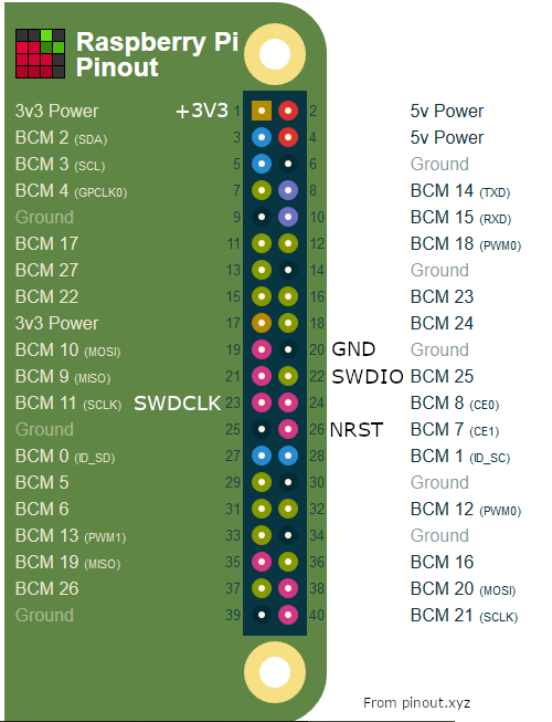
The guides, like the ones I linked in the beginning, use RPi pins (BCM) 18, 24 and 25 and a "native" OpenOCD configuration. I couldn't get that to work so I selected following pins that are used with a "sysfsgpio" configuration:
Raspberry Pi zero W pins used for SWD
To connected the boards together, I used some jumper wires, like shown in next figure.
Debug connection between the boards

OpenOCD configuration

The OpenOCD configuration was the most critical part! I had plenty of issues before I understood how to make the reset configuration. In the beginning, the flashing worked fine but the start address after reboot was wrong so the micro did start only randomly.

I needed to change the sysfsgpio-raspberrypi.cfg located at  /usr/share/openocd/scripts/interface/ to following:

#
# Config for using RaspberryPi's expansion header
#
# This is best used with a fast enough buffer but also
# is suitable for direct connection if the target voltage
# matches RPi's 3.3V
#
# Do not forget the GND connection, pin 6 of the expansion header.
#

interface sysfsgpio

# Each of the JTAG lines need a gpio number set: tck tms tdi tdo
# Header pin numbers: 23 22 19 21
sysfsgpio_jtag_nums 11 25 10 9

# Each of the SWD lines need a gpio number set: swclk swdio
# Header pin numbers: 23 22
sysfsgpio_swd_nums 11 25

# If you define trst or srst, use appropriate reset_config
# Header pin numbers: TRST - 26, SRST - 18

# sysfsgpio_trst_num 7
# reset_config trst_only

# sysfsgpio_srst_num 24
sysfsgpio_srst_num 7
reset_config srst_only srst_push_pull

# or if you have both connected,
# reset_config trst_and_srst srst_push_pull

The most important part was the sysfsgpio_srst_num 7 and reset_config srst_only srst_push_pull. With trst the reboot did not work properly. Only after I figured the correct reset config, did the micro start to reboot at the correct address at the beginning of flash memory!

Other thing was to do an OpenOCD config file openocd.cfg:
source [find interface/sysfsgpio-raspberrypi.cfg]
transport select swd
set WORKAREASIZE 0x2000
source [find target/stm32f0x.cfg]
reset_config srst_only srst_nogate
adapter_nsrst_delay 100
adapter_nsrst_assert_width 100
bindto 0.0.0.0
init
targets
reset halt
The first line tells to use the correct, already modified, interface configu. Then there is the source line telling the type of processor. And also in this config I have some reset config flags.

Also important line is the bind 0.0.0.0 which tells OpenOCD to allow connections from external interfaces (wifi). Otherwise only localhost is allowed, and the debugging over wifi won't work.

The OpenOCD must be started in the same directory where the openocd.cfg is located, with sudo opencd command.

Eclipse configuration

I won't go into details on how to configure Eclipse to be used with STM32, it was quite a pain in the ass to get to work. There are multiple guides on the 'net on the topic, one should follow those.

To get the OpenOCD debugger to work, I think I followed this guide. Most important part is to uncheck the "Start OpenOCD locally" setting, and fill in correct IP address and port of the RPi in the debug configuration.

Following figure shows the configuration I have.
Parameters for remote OpenOCD connection
Finally, here is a picture of the project I'm doing, running on mains power and the RPi enclosed inside the eclosure (top left corner). I can flash the firmware and debug all parameters etc. without any risk of electric shock!

Remote debugging the mains powered equipment

tiistai 4. joulukuuta 2018

Torque PIDs for Toyota Auris Hybrid

I have a 2017 model Toyota Auris Hybrid, and I like to monitor its status using an OBD-II bluetooth adapter and Torque Pro app on my Android phone. By default, the app only comes with a set of standard variables (PIDs, Parameter IDs), and to get any interesting data out of the car, some custom PIDs are needed.

Luckily, the Auris is quite close to Prius, and some guys at PriusChat forum have gathered a very comprehensive list of PIDs for Prius.

However, probably due to small differences in the cars quite large amount of those PIDs are not working and it is rather difficult to use since I never know beforehand which PID will work and which not. For this reason, I checked all the PIDs whether they work with Auris or not, and removed the non-working ones. I used the Prius list with latest change done 13.7.2014 as a base.

Here is the result csv. It has 212 items which are prefixed with "Auris-" to easily distinquish them from the standard PIDs. I think there might still be 1 or 2 that do not work, and IIRC I added battery power calculation that does not exist as a PID. With this list, it is very simple to do dashboards even without a connection to the car. Below is an example of a dashboard I made for testing.

It shows some basic information like GPS speed, battery state-of-charge and current, and ICE (gasoline engine) rotation speed. The graph shows the battery power limits together with the actual charge/discharge power (it works only with transparent theme, 3 graphs on top of each other).

The meters show coolant, catalysator, and battery temperatures.

On the bottom line there is indicators for ICE warm up request (if it is yes, the ICE will run until warm before the car can switch to EV mode automatically) and cruise control status with its setpoint (which is not normally shown in the dashboard, which is weird).

I've found the above information to be pretty good for normal driving. Other screens can be made for debuggin e.g. the battery condition. I also think about doing counters for energy regenerated and percent/distance driven in EV mode etc. Maybe I'll update the PID file if I get around to implement those.

Happy driving!